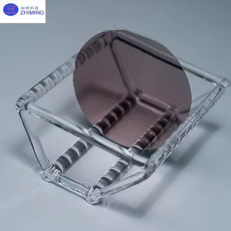
3inch/4inch/6inch/8inch Lithium Niobate Thin Film LNOI Wafers with Optical Loss <0.05 dB/cm
LNOI (Lithium Niobate on Insulator) wafers represent a high-performance integrated photonics substrate fabricated through advanced wafer bonding technologies (e.g., Smart Cut™ or direct bonding), integrating single-crystal LiNbO₃ thin films (100nm-1μm thickness) onto insulating substrates (such as SiO₂/Si or sapphire). ZMSH provides 4-inch, 6-inch, and custom-sized LNOI wafers supporting multiple crystal orientations (X-cut, Y-cut, Z-cut), with customizable film doping (e.g., MgO doping to enhance optical damage threshold) and buried oxide layer thickness (100nm-2μm). Substrate options include silicon, quartz, or silicon carbide to meet diverse optoelectronic integration needs. ZMSH offers comprehensive technical support from design to mass production, including film optimization, waveguide etching, and device-level testing services, enabling cutting-edge applications in high-speed optical communications and quantum computing.
Specification for X-cut Lithium Niobate on Insulator (LNOI) wafers
| S.N | Parameters | Specifications |
| 1 | LNOI wafer general specifications |
| 1.1 | Structure | LiNbO₃ / oxide / Si |
| 1.2 | Diameter | Φ100 ± 0.2 mm |
| 1.3 | Thickness | 525 ± 25 μm |
| 1.4 | Primary Flat Length | 32.5 ± 2 mm |
| 1.5 | Wafer Beveling | R Type |
| 1.6 | LTV | <1.5 μm (5×5 mm²)/95% |
| 1.7 | Bow | +/-50 μm |
| 1.8 | Warp | <50 μm |
| 1.9 | Edge Trimming | 2 ± 0.5 mm |
| 2 | Lithium Niobate layer specification |
| 2.1 | Average Thickness | 400 nm ± 10 nm |
| 2.2 | Orientation | X axis ±0.5° |
| 2.3 | Primary Flat Orientation | Z axis ±1° |
| 2.4 | Front Surface Roughness(Ra) | <1 nm |
| 2.5 | Bond Defects | >1 mm None;≤1 mm within 80 total |
| 2.6 | Front Surface Scratch | >1 cm None;≤1 cm within ≤3 total |
| 3 | Oxide (SiO2)layer specification |
| 3.1 | Thickness | 4700 ± 150 nm |
| 3.2 | Uniformity | ±5% |
| 4 | Si layer specification |
| 4.1 | Material | Si |
| 4.2 | Orientation | <100> ±1° |
| 4.3 | Primary Flat Orientation | <110> ±1° |
| 4.4 | Resistivity | >10 kΩ·cm |
| 4.5 | Backside | Etched |
| Notes:Valid/Latest authorization from OEM is required |

Key Features of LNOI Wafers
(1) Ultra-low optical loss: Waveguide propagation loss <0.05 dB/cm (1550nm band), 10× lower than conventional bulk LiNbO₃ devices.
(2) Strong electro-optic effect: Effective electro-optic coefficient (r₃₃) up to 90 pm/V (3× enhancement via optical field confinement), enabling ultra-low voltage modulation (Vπ~1V).
(3) High integration density: Supports sub-micron waveguides (width <1μm), reducing device footprint by 100× compared to bulk LiNbO₃.
(4) CMOS compatibility: Enables heterogeneous integration with silicon photonics (SiPh) and silicon nitride (SiN) platforms for multifunctional photonic chips.
(5) Thermal stability: Curie temperature up to 1140°C, suitable for high-temperature packaging processes.

Primary applications of LNOI Wafers
1. High-speed optical communications: LNOI's strong electro-optic effect makes it ideal for 200Gbps+ coherent optical modules, such as thin-film LiNbO₃ modulators (bandwidth >100GHz).
2. Quantum optics: Low-loss characteristics support entangled photon pair generation and quantum state manipulation for scalable quantum computing networks.
3. Microwave photonics: Combined with piezoelectric effects, enables optical phased arrays and microwave photonic filters (covering 5G/6G mmWave bands).
4. Nonlinear optics: High nonlinear coefficient (χ⁽²⁾) suitable for frequency combs and parametric amplification devices.
5. Sensing applications: Used in high-sensitivity biochemical sensors (e.g., silicon-based LNOI microring resonators).
ZMSH's Services
As a leading integrated photonics substrate provider, ZMSH delivers full-spectrum technical services covering the entire LNOI value chain, including customized thin film design (e.g., gradient-doped LiNbO₃), wafer-level bonding process development (supporting SiO₂, AlN, and other insulating layers), nanofabrication (EBL and IBE), and device-level performance verification (e.g., electro-optic response testing and THz characterization). ZMSH has achieved small-batch production of 6-inch LNOI wafers with >90% yield, and is collaborating with global research institutions to develop 8-inch LNOI and heterogeneous integration technologies (e.g., SiN-LNOI hybrid platforms). Future R&D focuses on reducing insertion loss (target <0.02 dB/cm) and enhancing modulation efficiency (r₃₃ optimization to 120 pm/V) to meet demands for 800G optical communications and quantum internet.

Q&A


